Scanning Electron Microscopy
Technique
SEM instruments measure the surface morphology of features within a range of millimetres to sub micrometres, by rastering an electron beam over the surface and detecting secondary electrons (SE) and backscatter electrons (BE). Both types of electrons carry information about the surface and material properties. In addition, quantitative and qualitative elemental analysis via Energy Dispersive Spectroscopy (EDS) provides further information on the material properties, enabling the generation of elemental maps that together with the surface image provides a whole set of key information, such as mineral composition in rocks, inclusions and distribution of components in alloys (Au/Pt), etc.
Instrument
Zeiss Leo 1455
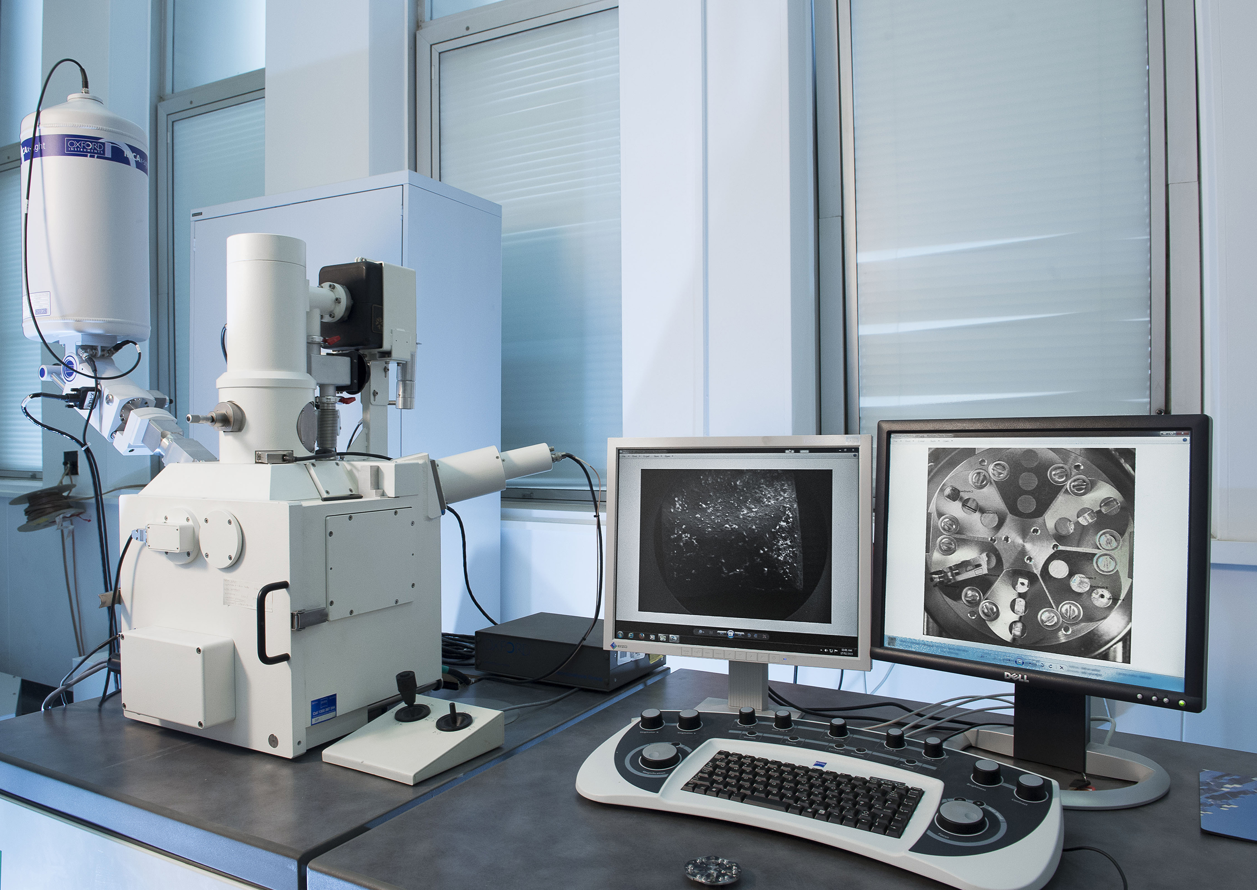
Equipped with:
- Thermal electron emission source (LaB6, Tungsten)
- Acceleration Voltage 5 - 30 keV
- Secondary Electron (SE) & Backscatter Electron (BE) Detector
- Energy Dispersive Spectroscopy (Oxford Inca).